1/5

Gallium Phosphide (GaP) Substrate / Wafer 2'' at Western Minmetals
$0.00
- FOB Price:
- Negotiable | Get Latest Price
- Order Quantity:
- 1 Set / Sets
- Supply Ability:
- 1000 Set / Sets per Month
- Port:
- shanghai
- Payment Terms:
- T/T L/C D/P D/A Credit Card PayPal Cash Escrow Other
- Delivery Detail:
- 5 days
Hot in store
-

High Purity Zinc 5N 6N 7N at Western Min
Inquiry -

High Purity Aluminum 6N 99.9999% at West
Inquiry -

High Purity Bismuth 5N 6N at Western Min
Inquiry -

High Purity Tin 5N 5N5 6N 7N at Western
Inquiry -

High Purity Antimony 5N 6N 7N at Western
Inquiry -

Epitaxial Single Crystal Silicon Wafer a
Inquiry -

Gallium Arsenide (GaAs) Zn-Doped Wafer a
$1.00 -

Gallium Phosphide (GaP) Substrate / Wafe
Inquiry
Product Details
Product Name: Gallium Phosphide (GaP) Substrate / Wafer 2'' at Western Minmetals Model NO.: 2'' Brand: WMC Application: LED Package: Aluminium Composite Type: Intrinsic Semiconductor Material: Gallium Phosphide Manufacturing Technology: VGF Diameter: 50.8+/-0.2mm Growth Method: Vgf Thickness: 300+/-20um Crystal Orientation: <111>+/-0.5degree Orientation Flat / Length: 16+/-1, 22+/-1 or 32+/-1 mm Identification Flat / Length: 8+/-1, 11+/-1 or 18+/-2 mm Orientation / Identification Flat Option: Ej, Us or Notch Resistivity: 0.003-0.3 Ohm.Cm Hall Mobility: 100 Cm2/V.S Min EPD: 3e5/Cm2 Trademark: WMC Transport Package: Wafer Container, Carton Box Outsiude Specification: 2'' Origin: Chengdu China HS Code: 8541900000 Product Description Gallium PhosphideSingle Crystal Wafer(GaP)is usually used for LED application.Diameter: 50.8+/- 0.2mmDopant: None / SulphurGrowthMethod: LECThickness: 300+/-20 umCrystal Orientation: <111>+/-0.5degreeOrientation Flat / Length: as SEMIIdentification Flat / Length: as SEMIOrientation / Identification FlatOption: as SEMICarrier Concentration: (4-6)E6 or (2-80)E17 /cm3Resistivity: 0.003-0.3 Ohm.cmHall Mobility: 100 cm2/v.s minFront / Backside Finish: P/P P/EEdge: no edge beveledProduct Packing: Aluminium CompositeTransportation Packing: wafer container, carton box outsiudeApplication: used for LEDNo.ItemStandard Specification1Size2"2Diametermm50.8±0.23Growth MethodLEC4DopedNoneor S5Conductor TypeSC/N6Standard Thicknessμm300±207Wafer Orientation<111>±0.5˚8ResistivityΩ.cm0.003-0.300Mobilitycm2/v.s100 minCarrier Concentrationcm-3(4-6)x106,(2-80)x1017, S-dopedEPDcm-2≤3x10⁵Front/Back SurfaceP/E, P/P, E/E, P/LEdge ProfileNo edge bevelParticle CountAs SEMI10Laser MarkBack side or upon request11PackagingSingle wafer container or cassetteWestern Minmetals (SC) Corporation isa major supplier of FZ or CZ 2-8inch single crystal (Monocrystal) silicon ingot and wafer, Neutron Transmutation Doping (NTD) silicon wafer, and semiconductor compoundssuch as VGF Gallium Arsenide (GaAs),Indium Phosphide (InP), Gallium Phosphide (GaP), Indium Antimonide (InSb) and Indium Arsenide (InAs) substrateetc for solar photovoltaic, integrated circuits, transistor and other electronic industry.It is our goal to be a consistent, reliable and an affordable source for our global clientsat any time.
Contact with Supplier
Recommend product
-
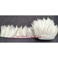
Stripped Soft Goose Fe
$3.00 -
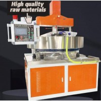
plastic ball grinding
$30000.00 -
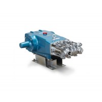
CAT piston pump 281
$4000.00 -
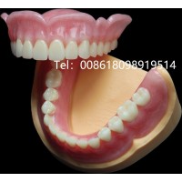
Droichead Zirconia Plu
$10.00 -
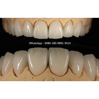
E.max crown, Veneer, I
Inquiry -
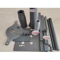
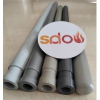
ReSiC Beams/plates/bur
$16.00 -
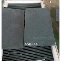
RSiC Slabs Boards Tile
$15.00 -
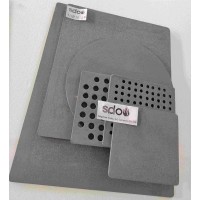
RSiC Batts as Kiln she
$15.00 -

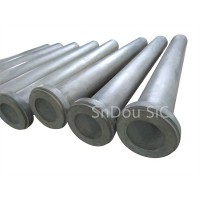
RSiC Tube by recrystal
$10.00 -
RSiC Kiln Furniture (B
$16.00 -
RSiC Burner Nozzle Fla
$18.00 -
RSiC Beam Support Pill
$16.00 -
RSiC plate Slab Board
$15.00 -

NSiC Tube Pipes by Nit
Inquiry -
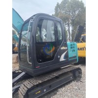
used excavator hudraul
$16600.00 -
NSiC Thermocouple Prot
Inquiry -

Stalk Riser Tube for L
Inquiry -
NSiC Ceramic Heater Pr
Inquiry -

RSiC NSiC Ceramic Kiln
Inquiry -
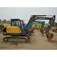
used excavator hudraul
$11500.00
Product parameters
closure
This shop is operated by agent
- Set up shop
- Authorized by Manufacturers & Suppliers online marketplace B2B platform GongWong.com, can provide agency service
- Service Introduction
- Authorized product, Internet cloud promotion service integrating certification promotion and procurement inquiry
- Intelligent website construction
- PC terminal + mobile terminal, create a cost-effective corporate website!
closure