1/5

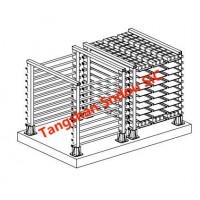
12 Layers High Tg 2.0mm PCB Printing
$110.00 / Square Met
- FOB Price:
- Negotiable | Get Latest Price
- Order Quantity:
- 1 Set / Sets
- Supply Ability:
- 1000 Set / Sets per Month
- Port:
- shanghai
- Payment Terms:
- T/T L/C D/P D/A Credit Card PayPal Cash Escrow Other
- Delivery Detail:
- 5 days
Hot in store
-

Multilayer PCB Half PTH Holes immersion
$60.00 -

Black Soldermask IC PCB
$60.00 -

2 Layer BGA Circuit PCB Board Printing
$65.00 -

High Thermal Metal Core Aluminium PCB
$65.00 -

3.2mm thickness 4layers High Tg PCB Boar
$110.00 -

12 Layers High Tg 2.0mm PCB Printing
$110.00 -

2.0mm Double Sided PCB
$60.00 -

2oz Aluminium OSP Circuit Board for LED
$65.00
Product Details
Product Name: 12 Layers High Tg 2.0mm PCB Printing Model NO.: Multilayer PCB-34 Customized: Customized Certification: RoHS, CCC, ISO, SGS base Material: FR-4 Layers: Multilayer metal Coating: Copper PP Thickness: 7628(0.18mm) 2116(0.12mm) 1080(0.08mm) Core base Board: 0.3mm 0.5mm 0.6mm 0.8mm 1.0mm Shipment: Air,Sea,Express(DHL TNT FedEx EMS UPS) Sample Date: 5-7days Trademark: ZAPON Transport Package: Vacuum Packing Specification: UL, TS16949, IPC 600 CLASS 2 Origin: China HS Code: 85340090 Product Description ZHEJIANG ZAPON ELECTRonIC TECHNOLOGY Co., Ltd is a professional manufacture of PCB and PCBA. Which have the factory of single side PCB, double side PCB, multi-layer PCB and PCB assembly etc. We have the ability of produce for any medium and mass quantity. The machine of our factory are on work all day and all night. With Zapon as a supplier, you will have the highest quality, quickest delivery.The products:Single-side PCB: CEM-1, FR-2, FR-1 XPC-94HBDouble-side PCB: FR-4, CEM-3, High Tg, Aluminum, Halogen FreeMulti-layer PCB: 4 to 22 layers(FR-4, High Tg, Rogers)Certification: UL, ISO9001, ISO/TS16949: 2002, IS014001 and RoHSTHE CAPACITY OF PRODUCTION: 50, 000SQM. /monthCapabilitiesNumber of LayersFrom 4-layer to 22- LayerMaterialFR-4,HighTg, RogersHalogen FreePCB ThicknessMin.thickness0.4mm(16mil)Max.thickness3.2mm(128mil)Surface finishedGold PlatingImmersion Gold(Silver)HAL Lead FreeHot Air Solder Leveling(HASL)Entek Coating (OSP)Solder MaskGreen,White,Black,Yellow,Red,BlueOther printingGold FingerCarbon Print, Peelable MaskSolder Mask Plugged HoleCopper thickness1/ 2 oz (18 μm) - 4 oz (140 μm)Min. Finished Hole Size0.2mm(8mil)Hole Size Tolerance (PTH)+/ -0.076mm (3 mil)Hole Size Tolerance (NPTH)+/-0.05mm (2 mil)Min. Line Width and Spacing0.1mm (4 mil)Min. Solder Mask Clearance0.05mm (2 mil)Min. Annular Ring0.076mm (3mil)Profile and V-CutCNC-Routing, Stamping and Beveling,V-CUT,CNCSpecial ProcessMicro-section, Chamfer for Gold Finger File format Gerber file, CAM350 ,Protel,PowerPCB E-TESTFlying Prob, E-test ,Fixture Other Test Impedance, Slice up Warp & Twist≤0.7%
Contact with Supplier
Recommend product
-
Stripped Soft Goose Fe
$3.00 -
plastic ball grinding
$30000.00 -
CAT piston pump 281
$4000.00 -
Droichead Zirconia Plu
$10.00 -
E.max crown, Veneer, I
Inquiry -
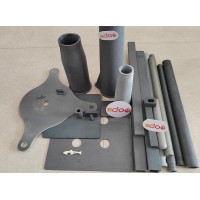
ReSiC Beams/plates/bur
$16.00 -
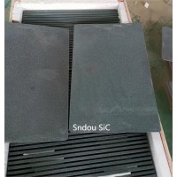
RSiC Slabs Boards Tile
$15.00 -
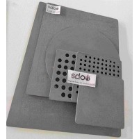
RSiC Batts as Kiln she
$15.00 -

RSiC Tube by recrystal
$10.00 -
RSiC Kiln Furniture (B
$16.00 -
RSiC Burner Nozzle Fla
$18.00 -
RSiC Beam Support Pill
$16.00 -
RSiC plate Slab Board
$15.00 -

NSiC Tube Pipes by Nit
Inquiry -
used excavator hudraul
$16600.00 -
NSiC Thermocouple Prot
Inquiry -

Stalk Riser Tube for L
Inquiry -
NSiC Ceramic Heater Pr
Inquiry -

RSiC NSiC Ceramic Kiln
Inquiry -
used excavator hudraul
$11500.00
Product parameters
closure
This shop is operated by agent
- Set up shop
- Authorized by Manufacturers & Suppliers online marketplace B2B platform GongWong.com, can provide agency service
- Service Introduction
- Authorized product, Internet cloud promotion service integrating certification promotion and procurement inquiry
- Intelligent website construction
- PC terminal + mobile terminal, create a cost-effective corporate website!
closure