1/5

UPS Control PCBA Board for LCD
$0.10 / Piece
- FOB Price:
- Negotiable | Get Latest Price
- Order Quantity:
- 1 Set / Sets
- Supply Ability:
- 1000 Set / Sets per Month
- Port:
- shanghai
- Payment Terms:
- T/T L/C D/P D/A Credit Card PayPal Cash Escrow Other
- Delivery Detail:
- 5 days
Hot in store
-
UPS Control PCBA Board for LCD
$0.10 -
SMT PCBA Board Assembly Multilayer PCBA
$0.50 -
Blue Solder Mask Bare PCB for PCB Assemb
$30.00 -
94V0 Flexible PCB/FPC Circuit Board
$30.00 -

Air Conditioner Circuit Board PCB
$0.10 -

High Quality and Technology OEM Circuit
$25.00 -

SMT LED PCB Board/China Flexible LED PCB
$30.00 -

Rigid-Flex PCB Flexible Printed Circuit
$30.00
Product Details
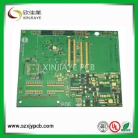
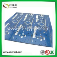
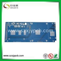
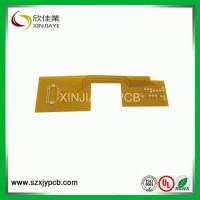
Product Name: UPS Control PCBA Board for LCD Model NO.: XJY-PCB 362 Brand: FPC Insulation Materials: Organic Resin base Material: Aluminum Processing Technology: Electrolytic Foil Mechanical Rigid: Fexible Flame Retardant Properties: V0 Material: Paper Phenolic Copper Foil Substrate Dielectric: Pi Type: Flexible Circuit Board Copper Thickness: 1/2 Oz Surface Finishing: Lf-Hal Solder Mask Type: Black Board Thickness: 1.0mm Min. Hole Size: 0.25mm Min Line Width: 0.075mm Layer: 1 to 24 Package: Vacuum Shipping: DHL, FedEx, UPS, Ect PCB: Circuit Board Trademark: oem Transport Package: Vacuum Package Specification: Normal Origin: China HS Code: 85340090 Product Description -----------Welcome to our website! ! XinJiaye is able to offer one stop 1 to 24 Layer PCB fabrication, PCB manufacturing, component sourcing,PCB Assembly, PCBA Test, Reverse engineering service; FPC fabrication, Aluminium base fabrication,High Frequency Board fabrica-tion.//////////////////////////////////////////////////////////////////////////////////////////////+++++Quick Detail++++++Place of Origin:Guangdong China (Mainland)Brand Name:XJYModel Number:xjy-pcb 362base Material:FR-4, Aluminum, Copper, Ceramic, Polyuret hane/MylarCopper Thickness:1/2 ozBoard Thickness:1.0mmMin. Hole Size:0.25mm (10mil)Min. Line Width:0.075mm (3mil)Surface Finishing:Lf-HalPCB:Circuit Board///////////////////////////////////////////////////////////////////////////////////////////////////////////////////////Technology capabilityItemsSingle/Double-sided Board/Multilayer Board/FPC(1-24Layer)base MaterialsFR-4(High TG 150°-170°),FR1,Aluminum,CEM-3,BT,94voFinish copper thicknessOuter 6 OZ,Inner 4 OZSurface finishENIG, ImAg, ImSn, OSP, HASL,Plating goldFinished Board SizeMax Double-sided Board640mm χ 1100mmMax Multilayer Board640mm χ 1100mmFinished Board Hole Size (PTHHole)Min Finished Board Hole Size0.15mmConductor Width and SpacingMin Conductor Width0.01mmMin Conductor Spacing0.01mmThickness of Plating and Coating LayerPTH Wall Copper Thickness>0.02mmTin Solder Thickness ( Hot Air Leveling )>0.02mmNickl/Gold ThicknessFor customer special needNickl Plating Layer>2umGold Plating Layer>0.3umBare Board TestSingle Side TestMax Test Point20480Max Board Test Size400mm χ 300mmDouble Side Test Max Test Point40960(General Use)4096(Special Use)Max Board Test Size406mmχ 325mm320mmχ 400mmMin Test pitch of SMT0.5mmTest Voltage10-250VMechanical Process Chamfer20°, 30°, 45°, 60°Angle Tolerance± 5°Deepness Tolerance± 0.20mmV-Cut Angle20°, 30°, 45°Board Thickness0.1-3.2mmResidues Thickness± 0.025mmCell Paraposition Precision± 0.025mmTolerance of Out-shape Process± 0.1mmBoard WarpMax Value0.7%Optical PlottingMax Plotting Area66mmχ 558.8mmPrecision± 0.01mmRepetitive Precision ± 0.005mmOur PCB board manufacture* PCB board file with parts list provided by customers* PCB board made, circuit board parts purchased by us* Electronic testing circuit board* Fast delivery, anti-static package* RoHS Directive-compliant, lead-freTesting Procedures For PCB Board---We perform multiple quality assuring procedures before shipping out any PCB board. These include:* Visual Inspection* Flying probe* Bed of nails· * Impedance control· * Solder-ability detection* Digital metallograghic microscope· *AOI (Automated Optical Inspection)Detailed Terms for PCB Manufacturing---Technical requirement for PCB assembly:* Professional Surface-mounting and Through-hole soldering Technology* Various sizes like 1206, 0805, 0603 components SMT technology* ICT(In Circuit Test), FCT(Functional Circuit Test) technology.* PCB Assembly With UL, CE, FCC, RoHS Approval* Nitrogen gas reflow soldering technology for SMT.* High Standard SMT&Solder Assembly Line* High density interconnected board placement technology capacity.Delivery Time for PCB board1) PCB production time: Sample: 3-4 days / mass production: Within 7 days2) Component purchase: 2 days if all components is available in our domestic market.3) PCB Assembly: Samples: Whthin 2 days / mass production: Within 5 daysQuotation Requirement://///////////////////////////////////////////////////////////////////////////////////////Following specifications are needed for quotation:A) base material:B) Board thickness:C) Copper thicknessD) Surface treatment:E) color of solder mask and silkscreen:F) QuantityShipping Method and Payment terms:1. By DHL, UPS, FedEx, TNT using clients account.2. We suggest you using our DHL, UPS, FedEx, TNT forwarder.3. By EMS (Usually for Russia Clients), price is high.4. By sea for mass quantity according to customer's requirement.5. By customer's Forwarder6. By Paypal, T/T, West Union, etc.Other Service:A) We have many special material as rogers, teflon, taconic, Fr-4 high tg, Ceramic in stock. Welcome to send us your inquiry.B) We also provide sourcing components, PCB design, PCB copy, PCB drawing, PCB assembly and so on.WELCOME TO ConTACT Betsy:
Contact with Supplier
Recommend product
-
Stripped Soft Goose Fe
$3.00 -
plastic ball grinding
$30000.00 -
CAT piston pump 281
$4000.00 -
Droichead Zirconia Plu
$10.00 -
E.max crown, Veneer, I
Inquiry -
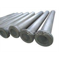
ReSiC Beams/plates/bur
$16.00 -
RSiC Slabs Boards Tile
$15.00 -
RSiC Batts as Kiln she
$15.00 -

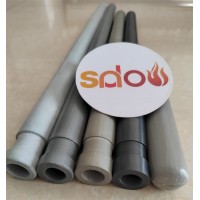
RSiC Tube by recrystal
$10.00 -
RSiC Kiln Furniture (B
$16.00 -
RSiC Burner Nozzle Fla
$18.00 -
RSiC Beam Support Pill
$16.00 -
RSiC plate Slab Board
$15.00 -

NSiC Tube Pipes by Nit
Inquiry -
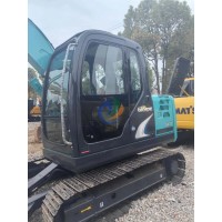
used excavator hudraul
$16600.00 -
NSiC Thermocouple Prot
Inquiry -

Stalk Riser Tube for L
Inquiry -
NSiC Ceramic Heater Pr
Inquiry -

RSiC NSiC Ceramic Kiln
Inquiry -
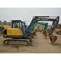
used excavator hudraul
$11500.00
Product parameters
closure
This shop is operated by agent
- Set up shop
- Authorized by Manufacturers & Suppliers online marketplace B2B platform GongWong.com, can provide agency service
- Service Introduction
- Authorized product, Internet cloud promotion service integrating certification promotion and procurement inquiry
- Intelligent website construction
- PC terminal + mobile terminal, create a cost-effective corporate website!
closure