1/5


China High Speed Cadence PCB Layout Design Services
$1.00 / pin
- FOB Price:
- Negotiable | Get Latest Price
- Order Quantity:
- 1 Set / Sets
- Supply Ability:
- 1000 Set / Sets per Month
- Port:
- shanghai
- Payment Terms:
- T/T L/C D/P D/A Credit Card PayPal Cash Escrow Other
- Delivery Detail:
- 5 days
Hot in store
-

High Quality Plated Through Hole PCB/Pth
$0.10 -

Prototype PCB Layout 94V0 Schematic Desi
$1.00 -

Customized 10 Hours High Quality PCB Des
$1.00 -

12 Hours High Quality Professional Pads
$1.00 -

China High Speed Cadence PCB Layout Desi
$1.00 -

Mentor Graphics Circuit Board PCB Design
$1.00 -

Fr4 Multilayer Electronics Appliances Fa
$0.10 -

Customized Multilayer Electonics PCB Man
$0.10
Product Details
Product Name: China High Speed Cadence PCB Layout Design Services Model NO.: pcbd20008 Type: Digital IC Technics: Thick Film IC Integration: SSIC Conductive Type: Unipolar Integrated Circuit Application: Standard Generalized Integrated Circuit shape: DIP Trademark: OEM Transport Package: Bubble Bag+Carton Specification: as custom required Origin: China HS Code: 39269090 Product Description SPEEDA Technology was founded in 2014, located in Changsha City, Hunan Province. It is an electronic technology company formed by a team with an average of 10+ years of electronic industry experience. The company is mainly engaged in the design, R&D(research and development), manufacturing and sales of various printed circuit boards. The products are widely used in communication equipment, computer and network equipment, consumer electronics, automotive electronics, industrial control, new energy, rail transit and other industries. We provide customers with "one-stop" service, that is, integrated service system consisting of printed circuit board circuit design optimization, small batch sample production, batch production and after-sale services. Adhere to quality first, service first, to improve customer satisfaction as the goal continuously.We are a leader in high-speed design and have in-depth research and technology accumulation for high-speed sheet and process.Our design types include high speed, simulation, digital-to-analog hybrid, high density, high voltage, high power, RF, backplane, ATE, soft board, soft and hard board, aluminum substrate and so on.We comprehensive check every procedure including principle design, DFM, DFT,High-speed, EMC, thermal design and so on.PCB Design ServiceIn the PCB layout, designers will consider different situations and use different design tools. The main factors to consider are:User interface (UI)PriceFeaturesLarge component libraryIntroduction of PCB DesignThe printed circuit board design is based on the circuit schematic diagram to realize the functions required by the circuit designer. The online PCB design mainly refers to layout design, which needs to consider various factors such as the layout of external connections, the optimal layout of internal electronic components, the optimal layout of metal wiring and through holes, electromagnetic protection, heat dissipation and so on. Excellent layout design can save production costs and achieve good circuit performance and heat dissipation performance. Simple layout design can be implemented manually, and complex layout design needs to be implemented with the aid of computer-aided design (CAD).An automated software program establishes a convenient method in PCB design that can be easily converted to a physical PCB. Listed below are some popular design tools such as Altium Designer, Eagle, and OrCAD.Commonly Used PCB Design SoftwareAltium Designer is more commonly used in China. This software is relatively simple and the design is more casual. It is not very good to use this software for complex PCBs.Cadence SPB, the ORCAD schematic design is an international standard; PCB design and simulation are very complete, which is more complicated to use than protel, mainly because the requirements and settings are complicated; Protel is obviously powerful.Mentor. The current MentorEE version is Mentor EE 7.9. It belongs to the same level of PCB design software as Cadence SPB. It is inferior to cadence SPB in some places. Its strengths are pulling wire and flying wire. It is called a flying wire king.EAGLE Layout This is the most widely used PCB design software in Europe.The PCB online design software mentioned above is used a lot, and Cadence SPB and MentorEE are well-deserved kings.Zuken's CADSTAR PCB design software provides a complete design environment. CADSTAR provides design capabilities throughout the PCB design process, from schematic to layout, routing, signal integrity simulation, power integrity analysis, and 3D mechanical integration.SPEEDAPCB Company AdvantageSPEEDAPCB's senior designers with rich design experience will provide one-to-one PCB design service for you, we can handle many different kinds of PCB circuit design, including high-frequency PCB design. And we will strive to satisfy customers. Reduce the number of R & D and the costs for you.Design delivery period and capabilityQuantityDelivery Time(working day)0-1000PIN1-3 days1000-3000PIN3-5 days3000-5000PIN5-7 days5000-8000PIN7-10 days8000-10000PIN10-13 days10000-20000PIN13-20 daysHighest layer of HDI20 layersHighest level HDIHDI any level of 24Highest layer of design52 layersMin line width2.5milMin line spacing2.5milMin hole size6mil(4mil laser drilling)Min BGA spacing0.35mmMax BGA-PIN3600PINHighest speed signal28GBPSPCB Design ProcessPCB Design ToolsFAQ:1.What are needed for quotation?A: PCB: Quantity, Gerber file and Technic requirements(material,surface finish treatment, copper thickness,board thickness ,...)PCbaservice: PCB information, BOM, (Testing documents...)Q2. What file formats do you accept for production?A: Gerber file: CAM350 RS274XPCB file: Protel 99SE, P-CAD 2001 PCBBOM: Excel (PDF,word,txt)Q3.Are my design files secure when I send them to you?A:Your files are never shared with any third parties, only our colleagues have access to your design files.Since they are your property, we respect the copyright of your files.Q4: What about OEM and ODM? and what is the MOQ?A: We accept both OEM and ODM orders..MOQ is 1 pcs.Q5: Delivery terms and time?A: We will ship the goods by DHL,TNT,Fedex,UPS or Aramex.the order can be sent out within 7-30 days depend on your order quantity, customization.Q6.Shipping cost?A: The shipping cost is determined by the destination, weight, packing size of the goods. Please let us know if you need us to quote you the shipping cost.Q7. Packing?A: Flexible packing according to the specific requirements of the clients.Q8.Payment?A: T/T,Western Union.Paypal.
Contact with Supplier
Recommend product
-
Stripped Soft Goose Fe
$3.00 -
plastic ball grinding
$30000.00 -
CAT piston pump 281
$4000.00 -
Droichead Zirconia Plu
$10.00 -
E.max crown, Veneer, I
Inquiry -
ReSiC Beams/plates/bur
$16.00 -
RSiC Slabs Boards Tile
$15.00 -
RSiC Batts as Kiln she
$15.00 -

RSiC Tube by recrystal
$10.00 -
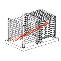
RSiC Kiln Furniture (B
$16.00 -
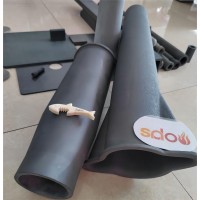
RSiC Burner Nozzle Fla
$18.00 -
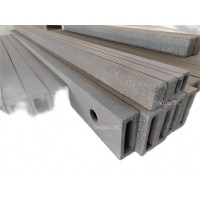
RSiC Beam Support Pill
$16.00 -
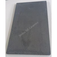
RSiC plate Slab Board
$15.00 -

NSiC Tube Pipes by Nit
Inquiry -
used excavator hudraul
$16600.00 -
NSiC Thermocouple Prot
Inquiry -

Stalk Riser Tube for L
Inquiry -
NSiC Ceramic Heater Pr
Inquiry -

RSiC NSiC Ceramic Kiln
Inquiry -
used excavator hudraul
$11500.00
Product parameters
closure
This shop is operated by agent
- Set up shop
- Authorized by Manufacturers & Suppliers online marketplace B2B platform GongWong.com, can provide agency service
- Service Introduction
- Authorized product, Internet cloud promotion service integrating certification promotion and procurement inquiry
- Intelligent website construction
- PC terminal + mobile terminal, create a cost-effective corporate website!
closure