1/5

2019 Top-Rated USB Adaptor Board PCBA
$0.10 / Pieces
- FOB Price:
- Negotiable | Get Latest Price
- Order Quantity:
- 1 Set / Sets
- Supply Ability:
- 1000 Set / Sets per Month
- Port:
- shanghai
- Payment Terms:
- T/T L/C D/P D/A Credit Card PayPal Cash Escrow Other
- Delivery Detail:
- 5 days
Hot in store


Product Details
Product Name: 2019 Top-Rated USB Adaptor Board PCBA Condition: New Customized: Customized Certification: RoHS, CCC, ISO, Ce, Reach base Material: FR-4 Layers: Multilayer Mode of Production: SMT by Machine, DIP by Hand metal Coating: Gold Product Name: PCBA PCB Copper Thickness: 1/3oz~7oz Surface Treatment: Ni/Au Plating Trademark: JIUDU Transport Package: Vacuum and Anti-Static Specification: PCBA Origin: Suzhou, Jiangsu Province, China HS Code: 8534001000 Product Description 2019 Top-rated USB Adaptor Board PCBA PCB CapacityNoItemsCapability1PCBLayers2 ~15 layers2PCBbase MaterialFR4, High Tg FR4, Halogen Free, Isola, Rogers, Aluminium3PCBFinished Board Thickness0.2mm ~7.0mm(8mil-276mil)4PCBCopper Thickness1/3oz ~7oz5PCBSurface FinishingHASL, Lead Free HASL, Immersion tin, Immersion gold, Gold plating, Immersion silver, OSP, Carbon, etc.6PCBMax gold plating thickness50 microinch7PCBMin. Trace Width/Space0.075/0.075mm(3/3mil)8PCBMin. Finish Holes Size0.1mm(4mil) for laser holes; 0.2mm(8mil) for mechanical holes9PCBMax.Finshed Size600mm x900mm (23.6" x35.43")10PCBHole TolerancePTH:±0.076mm(+/-3mil), NTPH:±0.05mm(+/-2mil)11PCBSoldermask ColorGreen, White, Black, Red, Yellow, Blue,12PCBSilkscreen ColorWhite, Black, Yellow, Blue13PCBImpedance Control+/-10%14PCBProfiling PunchingRouting, V-CUT, Chamfer15PCBSpecial HolesBlind/Buried holes, Countersunk holes16PCBReference StandardIPC-A-600H Class 2, Class 3, TS1694917PCBCertificateUL, ISO9001, ROHS, SGS18PCBPackageVacuum &CartonPCBA CapacityNOItemsCapability1PCB AssemblyMin. IC Pitch0.30mm(12mil)2PCB AssemblyFoot PinSO, SOP, SOJ, TSOP, TSSOP, QFP, BGA and U-BGA3PCB AssemblyMin. Chip Placement010054PCB AssemblyMax. PCB Size410mm x600mm(16.2" x23.6")5PCB AssemblyMin. PCB Thickness0.35mm(13.8mil)6PCB AssemblyMaximum BGA Size74mm x74mm(2.9" x2.9")7PCB AssemblyBGA Ball Pitch1mm ~3mm(4mil ~12mil)8PCB AssemblyBGA Ball Diameter0.4mm ~1mm(16mil ~40mil)9PCB AssemblyQFP Lead Pitch0.38mm ~2.54mm(15mil ~100mil)10PCB AssemblyPackageAnti-static Bubble Bag &CartonCompany InformationSince the setup of Jiudu, the company has devoted to PCB and PCBA development, constantly expanding the company's hardware equipment and improving its technical strength. The quality concept of "continuous improvement, pursuit of perfect quality, complete meeting customer needs" makes abroad customer base and agood reputation in the industry. It's business related to double-sided PCB and high precise multi-sided board(300000 feet/month), SMT(eight line), DIP(four line)automatic wave soldering, finished product assembly, etc, can provide customer with OEM and ODM one-stop fast delivery service.Factory GlanceOur ServiceInquiry1. Please send the BOM list and PCB Gerber files to us for detail quotation2. If you need to design, please provide us the schematic, functions of product, size etc. Sample and Picture would be better.Quotation1. Engineer confirms PCB requirements and Purchasing department confirms components.2. Quotation will be offered within 3working days.PaymentRegarding payment term: T/T, L/C, Western Union, PaypalSample makingA few samples will be produced before full production; all steps are strictly performed by company control and quality control.Mass ProductionAfter sample confirmed discussion about packing, shipping. Production department start the order schedule.Our EquipmentPackaging &Shippingabout packingFor PCBFor PCBAInner packing:Vacuum and Anti-static bubble bag.Outer packing:5-layer ultra hard High standard cartons box.Delivery Details:Sample5-7 days, Mass: 15-25daysabout shippingFAQQ1: What files do you use in PCB fabrication?A1: Gerber, pcb. Auto CADQ2: How do you make sure the quality?A2: Our Product is all 100% tested including Flying Probe Test (for sample), E-test (mass) or AOI.Q3: Can we visit your company?A3: Of course! Welcome to visit our company, JIUDU is located in Suzhou Industrial Park, Jiangsu province, china.Q4: What is the lead time?Q4: It takes 3-5 working days for sample, 7-10 working days for batch production based on files and quantity.Q5: Will you keep our information and files secret?A5: Sure! It is our basic principle to keep business secrets to protect our customers' rights and behalf.Q6. How to work with you?A6:-Email and send us the PCB layout file, BOM list- We will provide reply confirmation within 12 hours and reply to the offer within 3-5 days.- Waiting for your company to confirm the price, order and payment method.- We will start the production.Contact InfoMs WinnieJiudu Electronic Technology (Suzhou) Co., LtdCell: 86-18062117672/19947559620Website:www.jiudu-tech.comAdd:No. 96 Weixi Road, Sip, Suzhou, Jiangsu, China 215024
Contact with Supplier
Recommend product
-
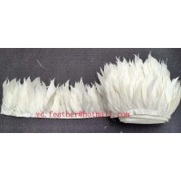
Stripped Soft Goose Fe
$3.00 -
plastic ball grinding
$30000.00 -
CAT piston pump 281
$4000.00 -
Droichead Zirconia Plu
$10.00 -
E.max crown, Veneer, I
Inquiry -
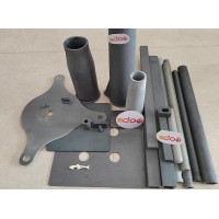
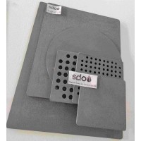
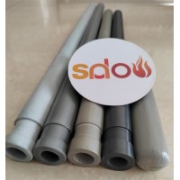
ReSiC Beams/plates/bur
$16.00 -
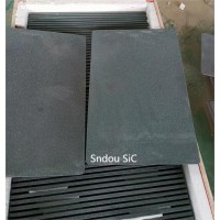
RSiC Slabs Boards Tile
$15.00 -
RSiC Batts as Kiln she
$15.00 -

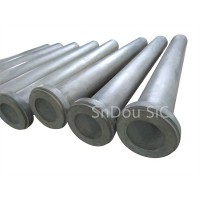
RSiC Tube by recrystal
$10.00 -
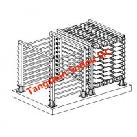
RSiC Kiln Furniture (B
$16.00 -
RSiC Burner Nozzle Fla
$18.00 -
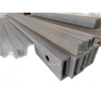
RSiC Beam Support Pill
$16.00 -
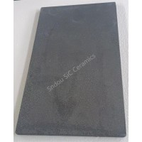
RSiC plate Slab Board
$15.00 -

NSiC Tube Pipes by Nit
Inquiry -
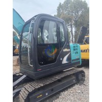
used excavator hudraul
$16600.00 -
NSiC Thermocouple Prot
Inquiry -

Stalk Riser Tube for L
Inquiry -
NSiC Ceramic Heater Pr
Inquiry -

RSiC NSiC Ceramic Kiln
Inquiry -
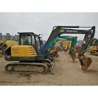
used excavator hudraul
$11500.00
Product parameters
closure
This shop is operated by agent
- Set up shop
- Authorized by Manufacturers & Suppliers online marketplace B2B platform GongWong.com, can provide agency service
- Service Introduction
- Authorized product, Internet cloud promotion service integrating certification promotion and procurement inquiry
- Intelligent website construction
- PC terminal + mobile terminal, create a cost-effective corporate website!
closure