1/5
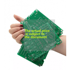


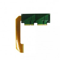
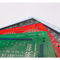
High Frequency Multilayer Flexible PCB
$80.00 / square met
1square met (MOQ)
- FOB Price:
- Negotiable | Get Latest Price
- Order Quantity:
- 1 Set / Sets
- Supply Ability:
- 1000 Set / Sets per Month
- Port:
- shanghai
- Payment Terms:
- T/T L/C D/P D/A Credit Card PayPal Cash Escrow Other
- Delivery Detail:
- 5 days
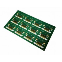
Hot in store
-
Rigid-Flex Board PCB RoHS Medical Flex B
$1.00 -
SMT Assembly Rigid Double-Layers Fr4 Cir
$1.00 -
Professional Smart PCB and PCBA for Pres
$1.00 -
OSP Aluminum PCB Board Metal Base PCB
$1.00 -
Aluminum Base PCB&PCBA Metal Core PCB Pr
$1.00 -
Professional Single and Double Sided Fle
$1.00 -
High Quality Multilayer Customized Print
$1.00 -
High Quality Double-Sided Printed Circu
$1.00
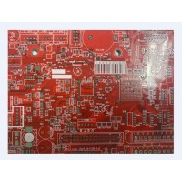
Product Details
| PCB Manufacturing Capabilities: | |
| Layers | 1-20 Layers |
| Laminate | FR4, H-TG, CEM, Aluminum, Copper base, Rogers, |
| Ceramics, Iron base | |
| Max. Board Size | 1200*480mm |
| Min.Board Thickness | 2-Layer 0.15mm |
| 4-Layer 0.4mm | |
| 6-Layer 0.6mm | |
| 8-Layer 1.5mm | |
| 10-Layer 1.6-2.0mm | |
| Min. Line Width/Trace | 0.1mm(4mil) |
| Max. Copper Thickness | 10 OZ |
| Min. S/M Pitch | 0.1mm(4mil) |
| Max. S/M Pitch | 0.2mm(8mil) |
| Min. Hole Dia. | 0.2mm(8mil) |
| Hole Dia. Tolerance(PTH) | ±0.05mm(2mil) |
| Hole Dia. Tolerance(NPTH) | ±0.05mm(2mil) |
| Hole Position Deviation | ±0.05mm(2mil) |
| Outline Tolerance | ±0.1mm(4mil) |
| Twist/Bent | 0.75% |
| Insulation Resistance | >1012Ω Normal |
| Electric Strength | >1.3kv/mm |
| S/M Abrasion | >6H |
| Thermal Stress | 288ºC 10Sec |
| Test Voltage | 50-300V |
| Min. Blind/Buried Via | 0.15mm(6mil) |
| Surface Treatment | OSP,HASL,LF-HASL,ENIG,Gold/Au Plating,Immersion Ag/Silver, |
| Ag/Silver Plating,Immersion Tin,Tin Plating | |
| Testing | E-test, Fly probe test |
Contact with Supplier
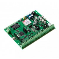
Recommend product
-
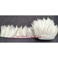
Stripped Soft Goose Fe
$3.00 -
plastic ball grinding
$30000.00 -
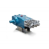
CAT piston pump 281
$4000.00 -
Droichead Zirconia Plu
$10.00 -
E.max crown, Veneer, I
Inquiry -
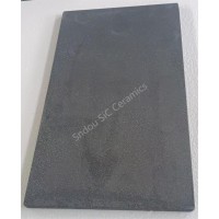
ReSiC Beams/plates/bur
$16.00 -
RSiC Slabs Boards Tile
$15.00 -
RSiC Batts as Kiln she
$15.00 -

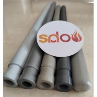
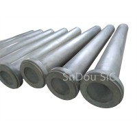
RSiC Tube by recrystal
$10.00 -
RSiC Kiln Furniture (B
$16.00 -
RSiC Burner Nozzle Fla
$18.00 -
RSiC Beam Support Pill
$16.00 -
RSiC plate Slab Board
$15.00 -

NSiC Tube Pipes by Nit
Inquiry -
used excavator hudraul
$16600.00 -
NSiC Thermocouple Prot
Inquiry -

Stalk Riser Tube for L
Inquiry -
NSiC Ceramic Heater Pr
Inquiry -

RSiC NSiC Ceramic Kiln
Inquiry -
used excavator hudraul
$11500.00
Product parameters
- brand:
- SY
closure
This shop is operated by agent
- Set up shop
- Authorized by Manufacturers & Suppliers online marketplace B2B platform GongWong.com, can provide agency service
- Service Introduction
- Authorized product, Internet cloud promotion service integrating certification promotion and procurement inquiry
- Intelligent website construction
- PC terminal + mobile terminal, create a cost-effective corporate website!
closure